25 W AUDIO AMPLIFIER MOSFET IRF530-IRF9530

25 W AUDIO AMPLIFIER MOSFET IRF530-IRF9530
The supply rails prudentially voltage was kept at the rather low value of + and - 32V.

Note:

  • Q6 & Q7 must have a small U-shaped heatsink.
  • Q8 & Q9 must be mounted on heatsink.
  • Adjust R11 to set quiescent current at 100mA (best measured with an Avo-meter connected in series to Q8 Drain) with no input signal.
  • A correct grounding is very important to eliminate hum and ground loops. Connect to the same point the ground sides of R1, R4, R9, C3 to C8. Connect C11 to output ground. Then connect separately the input and output grounds to power supply ground.

»»  read more

20 W CLASS-A POWER AMPLIFIER CIRCUIT DIAGRAM

20 W CLASS-A POWER AMPLIFIER CIRCUIT DIAGRAM
The current sink shown should have very high linearity, since it is based on the same concept as the output stage devices. The 0.25 Ohm resistor should cause little grief (4 x 1 Ohm 1W resistors in parallel), but some experimentation may be needed here, since the base-emitter voltage of the BC549 determines the current. This circuit works by using the BC549 to steal any excess base current from the compound pair. As soon as the voltage across the 0.25 Ohm resistor exceeds 0.65V, the transistor turns on and achieves balance virtually instantly.

The 1k trimpot in the collector of the first LTP transistor allows the DC offset to be adjusted. The nominal value is around 400 ohms, but making it variable allows you to set the output DC offset to within a few mV of zero.

»»  read more

14 W AUDIO AMPLIFIER TDA2030 CIRCUIT SCHEMATIC DIAGRAM

14 W AUDIO AMPLIFIER TDA2030 CIRCUIT SCHEMATIC DIAGRAM
Resistors should be at least 1/4W types with 1% tolerance recommended. I used 0.6W 1% metal film resistors and they work well. Capacitors I used were electrolytic cans for C2, C5 and C6. At the time of building, I did not have enough 100uF caps so I used 220uF caps instead, this will not cause trouble, unless you use caps that are smaller than 100uF for C5 and C6.

C1 can be electrolytic, I used a tantalum myself (don't ask why, since they are actually more expensive). Some readers may want to use a polyester capacitor for the input (C1), this would work too but I am not sure whether any benefit will arise from the extra expense. Other capacitors (bypass caps C3 and C4. and C7) are ideally polyester caps. Mylar may be used but I prefer polyester caps and they are not expensive unless you get large values.

The values of R5 and C8 are worked out from the equations in the datasheet, but I used 1.8k ohm for R5 and 220pF for C8 and they work fine. Diodes should be 1N4001 or similar (make sure you solder them in the right way round).

A good heatsink is important and this should be a large size with good thermal conductivity. When you operate the TDA2030 from the (recommended) split rail power supply, you must insulate the device from the heatsink using a mica washer or similar. With single rail supply, this is not needed.

»»  read more

14W CLASS A AMPLIFIER CIRCUIT USING 2N3055 SCHEMATIC DIAGRAM

14W CLASS A AMPLIFIER CIRCUIT USING 2N3055 SCHEMATIC DIAGRAM
Many early amplifiers operated in Class A, but as output powers rose above 10W the problems of heat dissipation and power supply design caused most manufacturers to turn to the simpler, more efficient Class B arrangements and to put up with the resulting drop in perceived output quality. Why Class A ? Because , when biased to class A, the transistors are always turned on, always ready to respond instantaneously to an input signal. Class B and Class AB output stages require a microsecond or more to turn on. The Class A operation permits cleaner operation under the high-current slewing conditions that occur when transient audio signal are fed difficult loads. His amplifier is basically simple, as can be seen from the block diagram.

»»  read more

12 VOLT AUDIO AMPLIFIER USING TRANSISTOR CIRCUIT DIAGRAM

12 VOLT AUDIO AMPLIFIER USING TRANSISTOR CIRCUIT DIAGRAM
Closing SW1 a bass-boost is provided but, at the same time, volume control must be increased to compensate for power loss at higher frequencies. In use, R9 should be carefully adjusted to provide minimal audible signal cross-over distortion consistent with minimal measured quiescent current consumption; a good compromise is to set the quiescent current at about 10-15 mA.To measure this current, wire a DC current meter temporarily in series with the collector of Q3.

List Component

P1_____________10K Log.Potentiometer
R1,R2__________33K 1/4W Resistors
R3_____________33R 1/4W Resistor
R4_____________15K 1/4W Resistor
R5,R6___________1K 1/4W Resistors
R7____________680R 1/4W Resistor
R8____________120R 1/2W Resistor
R9____________100R 1/2W Trimmer Cermet
C1,C2__________10µF 63V Electrolytic Capacitors
C3____________100µF 25V Electrolytic Capacitor
C4,C7_________470µF 25V Electrolytic Capacitors
C5_____________47pF 63V Ceramic Capacitor
C6____________220nF 63V Polyester Capacitor
C8___________1000µF 25V Electrolytic Capacitor
D1___________1N4148 75V 150mA Diode
Q1____________BC560C 45V 100mA PNP Low noise High gain Transistor
Q2____________BC337 45V 800mA NPN Transistor
Q3____________TIP31A 60V 4A NPN Transistor
Q4 ___________TIP32A 60V 4A PNP Transistor
SW1___________SPST switch

»»  read more

12 VOLT AUDIO AMPLIFIER IC TDA7222AP CIRCUIT DIAGRAM

12 VOLT AUDIO AMPLIFIER IC TDA7222AP CIRCUIT DIAGRAM

Note

Use 12V DC for powering the circuit.
The IC must be heatsinked.
Speaker can be a 4 ohms one.
For optimum performance input and output must be separately grounded.

Pin Name Description
1 Vcc Supply Voltage
2 RR Ripple Reject
3 MC Muting control
4 OP AF Signal Input
5 FB FB Filter
6 GA Gain adjust
7 GND Ground
8 GND Ground
9 OP AF Output
10 BS BootStrap
»»  read more

10 WATT AUDIO AMPLIFIER WITH BASS-BOOST CIRCUIT DIAGRAM

10 WATT AUDIO AMPLIFIER WITH BASS-BOOST CIRCUIT DIAGRAM

Note:
This circuit can be connected directly to a CD player, tuner, and tape recorders.
Transistor Q3 and Q4 must be in pairs with the heatsink.

Adjust the volume control on the minimum and R3 position with a minimum value of resistance as well. try to switch the circuit set in R3 to read the flow of about 20 to 25mA. Wait for 15 minutes, connect the ground of A1, P1, C2, C3dan C4. Connect the output also C9 ground

List Component

P1 : 22K Log Potemsiometer (Dual gang for stereo)
C3, 4 : 470uF/25V
P2 : 100K Log Potemsiometer (Dual gang for stereo)
C6 : 47pF 63V ceramic ar polyester capasitor
R2, 4, 8 : 820R 1/4W
C7 : 10nF 63V polyester capasitor
R1 : 4K7 1/4W
C9 : 100nF 63V polyester capasitor
R3 : 500R 1/2W
D1 : 1N4148 75V 150mA Diode
R5 : 82K 1/4W
IC 1 : NE5532 Low noise Dual Op-amp
R6, 7 : 47K 1/4W
Q1 : BC547B 45V 100mA NPN Transitor
R9 : 10R 1/2W
Q2 : BC557B 45V 100mA PNP Transitor
R10 : 0,22 4W(wirewound)
Q3 : TIP42A 60V 6A PNP Transistor
C1, 8 : 470nF 63V polyester capasitor
Q4 : TIP41A 60V 6A NPN Transistor
C2, 5 : 100uF/25V J1 : RCA audio input socket

»»  read more

9 VOLT HEADPHONE AMPLIFIER NE5534 SCHEMATIC DIAGRAM

9 VOLT HEADPHONE AMPLIFIER NE5534 SCHEMATIC DIAGRAM
The NE5532 is a very convenient package of two 5534s in one 8-pin devices with internal unity-gain compensation, as there are no spare pins. The 5534/2 is a low-distortion, low-noise device, having also the ability to drive low-impedance loads to a full voltage swing while maintaining low distortion. Furthermore, it is fully output short-circuit proof. Therefore, this circuit was implemented with a single NE5532 chip forming a pair of stereo, inverting amplifiers, having an ac gain of about 3.5 and capable of delivering up to 3.6V peak-to-peak into a 32 Ohm load (corresponding to 50mW RMS) at less than 0.025% total harmonic distortion (1kHz & 10kHz).

I have Used it with Sennheiser 465s and achieved ear-splitting volume. The amplifier is ideal as a booster for power-conserving stereo sources Such as portable CD players and for interfacing with passive EQ networks Such as tone controls or a headphone acoustic simulator.


»»  read more

4 x 25 W CAR AMPLIFIER TDA7381 SCHEMATIC DIAGRAM

4 x 25 W CAR AMPLIFIER TDA7381 SCHEMATIC DIAGRAM

The TDA7381 is a class AB audio power amplifier in Flexiwatt25 package designed for car radio applications. You you can also use this circuit for other purposes. Thanks to the fully complementary PNP/NPN output configuration the TDA7381 allows a rail to rail output voltage swing with no need of bootstrap capacitors.

The extremely reduced components count allows very compact sets. The on-board clipping detector simplifies gain compression operations. The fault diagnostics makes it possible to detect mistakes during Car- Radio assembly and wiring in the car.

Absolute maximum ratings of IC TDA7295 IC

  • Operating supply voltage = 18 V
  • DC supply voltage = 28 V
  • Peak supply voltage (t = 50 ms) = 50 V
  • Output peak current Repetitive (duty cycle 10 % at f = 10 Hz) = 3 A
  • Output peak current Non repetitive (t = 100 µs) = 4A
  • Power dissipation, (Tcase = 70 °C) = 80 W
  • Junction temperature = 150 °C
  • Storage temperature = -40 to 150 °C

»»  read more

3 VOLT - 6 VOLT MINI AUDIO AMPLIFIER SCHEMATIC DIAGRAM

3 VOLT - 6 VOLT MINI AUDIO AMPLIFIER SCHEMATIC DIAGRAM

The potentiometer circuit can be used to control volume. Capacitor C1 and C2 are designed to filter supplyvoltage If the battery separator is used as operations offer source.For using batteries C1 and C2 are not required.

IC TDA7052 is a mono output amplifier in 8-comng Head DI package (DIP). The device is designed primarily for battery-operated portable audio circuits. Features include TDA 7052, no external components needed, no switch-on or switch-off button sounds great overall stability and very low power consumption (quiescent current of 4 mA), low THD, it is not necessary any cooler and short-circuit proof.

Profit TDA 7052 is set internally at 40 dB. . Compensate for the reduction of output power due to low voltage TDA7052 uses Bridge-Tied-Load principle
(BTL), which can provide power about 1 to 2 W RMS (THD = 10%), 8 ohm load to the power supply 6 V.

»»  read more

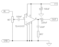
0.5 WATT MINI AMPLIFIER TDA1015T SCHEMATIC DIAGRAM

0.5 WATT MINI AMPLIFIER TDA1015T SCHEMATIC DIAGRAM
A volume control is included in schematic. Log type is required and 4k7 to 10k is about right. A dual pot is needed if you plan on using two TDA1015's to complete a stereo amp.

Chances are you'll want this amplifier portable. Batteries do the trick fine, but you won't get much power out of a couple of 1.5V cells. Unfortunately the size of a decent amount of battery power will mean that the overall size of this amp will be much bigger and for that there are more benefits to be had using a device like the TDA7052 or TDA2822 for stereo.

Quick ref data of TDA1015T Chip

  • Supply voltage range: 3,6 to 12 V
  • Peak output current: 1 A
  • Output power: 0,5 W
  • Voltage gain power amplifier: 29 dB
  • Voltage gain preamplifier: 23 dB
  • Total quiescent current: 22 mA
  • Operating ambient temperature range: -25 to +150 °C
  • Storage temperature range: -55 to + 150 °C

»»  read more

other circuit